OCTSENS TECH CO., LTD.

Home            About Us            Content            NTC Thermistors              Light Sensors          E-mail

Construction Characteristics of Cds Cells

Photosensitive devices can be divided into photovoltaic devices and photo emissive devices. CdS cells are a type of photoconductive device. They are semiconductor sensors that utilize the photoconductive effect in which light entering the photoconductive surface reduces the resistance. A voltage is applied to both ends of a CdS cell and the change in resistance due to light is output as a current change signal. Despite of small size, the output current per photoconductive surface area is large enough to drive relays directly. For this reason, CdS cells are used in a wide variety of fields.


Here we will explain briefly the basic operating principles, fabrication and structure of CdS cells.

¡@

PHOTOCONDUCTIVE EFFECT

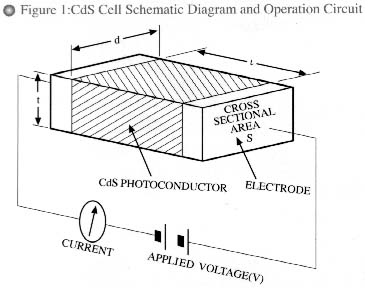
Figure 1 is a schematic diagram of a CdS cell and its operation circuit. An electrode is set at each end of the photoconductor. In darkness, the photoconductor resistance is very high, and when a voltage is applied, the ammeter shows only a small dark current. This is the CdS photoconductor's characteristic thermal equilibrium current. When light is incident on this photoconductor, a current (I) flows. Figure 2 shows the current that flows when the amount of light is increased.


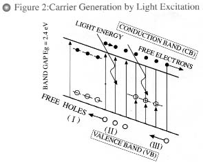
Here are the basic principles of the photoconductive effect.

(  £L  ) Directly beneath the conduction band of the CdS crystal is a donor level and there is an acceptor level above the valence band. In darkness, the electrons and holes in each level are almost crammed in place in the crystal and the photoconductor is at high resistance.

(  £L£L  ) When light illuminates the CdS crystal and is absorbed by the crystal, the electrons in the valence band are excited into the conduction band. This creates pairs of free holes in the valence band and free electrons in the conduction band, increasing the conductance.

(  £L£L£L  ) Furthermore, near the valence band is a separate acceptor level that can capture free electrons only with difficulty, but captures free holes easily. This lowers the recombination probability of the electrons and holes and increases the number for electrons in the conduction band for N-type conductance.

The increase in conductance in ( £L£L ) requires that the light energy be greater than the bank gap Eg. For CdS with a bank gap of 2.41

eV, the absorption edge wavelength £f is

£f= c/ £o =hc/Eph=1240/Eg~515( nm )

Where Eph :photon energy (h £o )

                 h: Planck's constant

                 £o: light frequency

                 C: speed of light

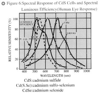
Therefore, the CdS crystal absorbs light with a wavelength shorter than 515 nm and lets light with a wavelength longer than

515 nm be transmitted. Therefore, the photoconductor's absorption edge wavelength determines the spectral response characteristic on the long 
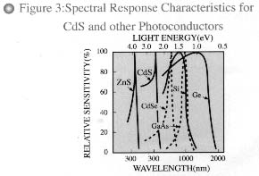
wavelength side. In the actual spectral response characteristic shown in Figure 3, the sensitivity of CdS drops at wavelengths shorter than 515 nm. This is because at short wavelengths, the light is absorbed near the surface of the crystal, increasing the local charge density and inducing electron hole recombination, and also because there are lattice defects at the crystal surface, they promote the recombination.

Until the carries generated in ( £L£L ) and ( £L£L£L ) recombine, electrons are injected from one electrode and pulled out by the other.

When these carriers last longer and they move more, the conductance increases greatly. The conductance £G p is given by the following equation.

£Gp=ef( £gn £nn+ £gp £np)

Where £gn, £gp: free electron, free hole movement (cm/V £» sec)

           £nn, £np: free electron, free hole life (sec)

                   f: number of generated carriers per

                second per cubic volume

For a CdS cell, £gn £nn>>£gp £np and conductance by free holes can be ignored. Then it becomes an N type semiconductor. Thus,

            £Gp=ef £» £gn £nn

Here, the gain G is defined as how many electrons flow between the electrodes due to excitation by one photon in the CdS photoconductor (until the carrier lifespan is over).

      G= £nn /tt

Where tt: tranist time between electrodes =£L2/V £gn

              £L: distance between electrodes

             V: voltage applied

Therefore,

G= £gn £nn V /£L2

If, for example, £gn=300 cm2/V £»sec, £nn=10-3 sec, 1=0.2mm, and 1.2V, then the gain is 900. This means that there is multiplication in the CdS photoconductor and that the CdS is highly sensitive.

    The sensitivity of CdS is the change in resistance, i.e. the change in current in response to change in light. As Figure 1 shows, if the distance between the electrodes is 1 the cross-sectional area of the photoconductor is S, and the voltage applied is V, then from Ohm's law:

£G£L¡Û£Gp.S£»V/1=£Gp£»t£» V/1

If the conductance  £Gp and the photoconductor thickness t are held constant, then,

£G£L¡Û d/1¡÷resistance ¡µ R ¡Û 1/d

This 1/d is an important factor in designing the electrode configuration. In other words, the shorter distance between the electrodes and the greater the electrode length, the higher the sensitivity and the lower the cell resistance. Thus, the electrode patterns for high-sensitivity CdS cells consist of many zig-zags.

STRUCTURE

The manufacturing process of the photoconductive layer into the sintered type, single crystal type and evaporated type can divide CdS cells. Of these different types the sintered type offers high sensitivity areas, a large mass production effect, and relatively superior production profitability, so AGI uses the sintering film fabrication method.

   Here is the process for making sintered CdS cells. Impurities and a fusing agent for encouraging crystal growth are added to highly pure CdS crystal power and this mixture is dissolved in water. The resulting solution is applied to CdS ceramic substrate and dried, and then it is sintered in a high-temperature oven to form multiple crystals. In this way, a thick layer with the photoconductive effect is formed.

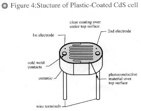
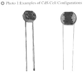
   Then, lead terminals are introduced to the CdS substrate and the CdS is packaged. (Figure 4 and photo 1 shows an example of the structure of a plastic-coated CdS cell.)


CHARACTERISTICS

In the selection of a suitable CdS cell, the characteristics required by the functions of the circuit in which the CdS cell is to be used are important; in general, there are analog uses such as light measurement and digital uses such as on-off switching.

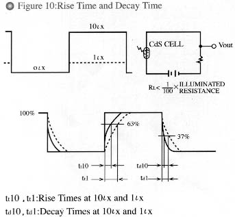
Use in digital circuits such as switching requires a fast response and a high ratio between illuminated resistance and dark resistance. For 
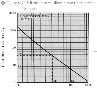
illumination and exposure meter and other devices that measure brightness, the sensitivity, the slope of the  resistance vs. illuminant (gamma), and the spectral response characteristic are important. Therefore, understanding the various characteristics of CdS cells presented below is important for selecting the night CdS cell for your application.

MAXIMUM RATINGS

The maximum ratings given in this catalog are absolute maximum ratings. This means that these are the values, which are not to be exceeded even momentarily. Values above the maximum rating may break down the CdS cell and lower its performance, so take adequate care in circuit design to avoid them.

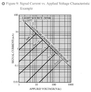
¡´ Allowable Power Dissipation

Allowable power dissipation is the limiting value of power consumption of a CdS cell when it is operated in a circuit. If a CdS cell is operated under conditions that cause its allowable power dissipation to exceed, deterioration of performance is hastened and the photoconductive surface can be damaged or broken down. Therefore, this parameter must be held within the ratings in the same manner, as are the applied voltage and ambient temperature. This allowable power dissipation applies to total illumination of the photoconductive surface of a CdS cell, so when only part of the surface is used, the allowable power dissipation must be reduced in proportion to the illuminated surface area.

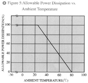
The allowable power dissipation figures in this catalog are for a temperature of 25¢J. 
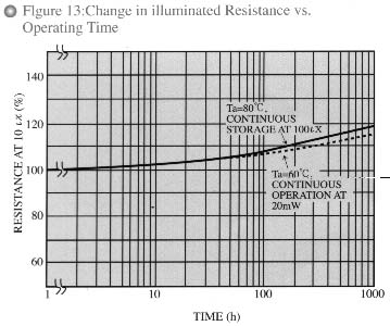
When these CdS cells are used at higher ambient temperatures, the power consumption must be reduced, as the dreading shown in Figure 5. So this point must be taken into consideration as well.

¡´ Ambient Temperature Range

Unless otherwise specified, the maximum rated ambient temperature range is for CdS cell operation and storage. Operating or storing a CdS cell outside of this temperature range reduces its performance. Never keep or operate Cds cells at temperature exceeding the maximum rating. It is suggested to keep CdS cells at normal room temperature and humidity before using them.

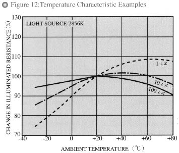
Even within the ambient temperature range, the cell resistance, response, and other characteristics vary somewhat with the temperature, so take this into consideration.

¡´ Applied Voltage

The maximum applied voltage is the voltage that can be applied between the two terminals of a CdS cell. When the CdS cell resistance is at its maximum (the equilibrium dark resistance in total darkness), the voltage that can be applied between the CdS cell terminals is also at its maximum. Never let the applied voltage exceed the maximum rating. If the power consumption increases during CdS cell operation, the rating of allowable power dissipation should take precedence over the applied voltage rating.

SENSITIVITY

¡´Spectral Response Characteristic

The relative sensitivity of a CdS cell is dependent on the wavelength of the incident light. The sensitivity as a function of wavelength is called the spectral response characteristic. Fundamentally, the maximum sensitivity wavelength (or peak wavelength) for CdS cell is 515 nm, but by controlling the composition ratio of CdS to CdSe, the maximum sensitively can be optimized at a wavelength between 515 and 730nm. So, photoconductive cells with spectral response close to that of the human eye are available.

Figure 6 shows these relationships. In general, CdS Cd (S¡DSe), and CdSe cells are all often called ¡§CdS cell ¡¨. This catalog also uses this terminology.

By using a CdS cell with a spectral response similar to the human eye, it can be widely and easily used in applications as sensors substituting for the human eye.

 ¡´Expressing Sensitivity

In general, the sensitivity of light sensors expresses the relation between the intensity of the light impinging on the sensitive surface and the resulting output signal. If voltage V is applied across a CdS cell and illuminant E (lux) is shone on it, and signal current IL flows, then

    IL=K¡DV£\E£^

where K is a constant, £\ is the voltage index for signal current and can be treated as just about 1, and  £^ (gamma) is also called the illuminant index for signal current and shows the slope of the signal current vs. illuminant characteristic.

As the above equation shows, the sensitivity can be expressed as the value of the signal current with respect to the incident illuminant, but usually, rather than expressed in the signal current; the sensitivity is expressed in the cell resistance.

REFERENCE

Lux is a unit of illuminant, equal to the illuminant on a surface

1 square meter in area on which there is a luminous flux of 1 lumen uniformly distributed. The illuminant is proportional to luminous intensity of the light source and is inversely proportional to the square of the distance from the light source.

Therefore, the illuminant E (lux) at distance D meters from a point light source of luminous intensity I (cd) am obtained from the equation:

All of this based on the standard luminous efficiency, so these are light measurement units for the visible region only.


The lux is a light measurement unit based on the standard lumious efficiency. Therefore, light sensors with spectral response characteristics, which are shifted from the standard luminous efficiency, show different output signals if the radiant spectral distribution (color temperature) of the light source is different, even if the illuminant is the same. Therefore, when using light sources for light measurement, the radiant spectral distribution characteristic must be specified.

At OCTSENS, a tungsten lamp with a color temperature of 2856K is used as the standard light source. The color temperature of the tungsten lamp is expressed as the absolute temperature of a black body (a platinum black body furnace), which is approximately proportional in the visible region to the spectral radiant distribution of the lamp


¡´Illuminant vs. Resistance

Figure 8 gives a typical example graphing the CdS cell resistance as a function of incident illuminant. The slope of this curve, £^ (gamma), varies with the cell type and is important for detecting analog-like light level differences. This £^ is given by the tangent £c of a line connecting two points on the curve, If the illuminated resistances at illuminant Ea(lux) and Eb(lux) are Ra( £[ ) and Rb( £[ ), then £^ between a and b is expressed by the following equation:

From this relationship, the conversion equation:

Ra=Rb x (Ea/Eb)-£^ab

is obtained. If the slope £^ab and the illuminated resistance Rb are known, the illuminated resistance for any point between Ea and Eb can be obtained. Also, this relationship gives the

equation:

Ea=Eb x (Ra/Rb)-1/£^ab

Given the value of £^ab and the illuminated resistance Rb at illuminant Eb, the illuminant Ea that will give an illuminated resistance of Ra can be obtained.

SIGNAL CURRENT VS. APPLIED VOLTAGE

Figure 9 shows the signal current vs. applied voltage characteristic for different illuminant levels. This characteristic is nearly linear and holds for applied voltages down to 1 V and less.

However, if a voltage is applied that brings the power consumption near the allowable power dissipation, the amount of heat generated by the CdS cell increases, causing a change in cell resistance, so this linearity is lost. Be aware of this point in designing.

¡´DARK RESISTANCE/DARK CURRENT

If a CdS cell is left in total darkness for 15 hours or so, then the value of its resistance is quite high by measured. This is true dark resistance (equilibrium dark resistance). In practical applications, however, the CdS cell is used at various light levels, so the previous light levels affect the dark resistance (this is called light history effect and will be described later). Therefore, the dark resistance must be expressed specifying the time allowed after the

Incident light is removed. In this catalog, the dark resistance is measured 10 seconds after incident light of 10 lux has been cut off. This dark resistance measurement can also be viewed as expressing the response time (decay time) for CdS cells.

RESPONSE SPEED

Cds cells have a certain time delay in responding to incident light. This response speed is an important point in designing detection of rapidly changing light levels and on-off switches.

The response speed is usually expressed as the time required for the illuminated resistance to reach 63% of its saturation value after the cell is illuminated (rise time), and as the time required for the illuminated resistance to decay to 37% of its saturation value after the light is removed (decay time) The rise and decay times listed in this catalog are measured with repetitive intermittent light.

The response speed varies considerably with the light level, the light history condition, the load resistance, the ambient temperature, and other factors. The higher the incident lights level, the faster the response speed. Also, cells kept in darkness exhibit slower response than cells kept at a brighter light level, and this effect becomes more distinct as the cell is kept for longer periods at a dark light level. Also, the apparent rise time becomes faster with a larger load resistance, but the decay time shows the contrary effect.

LIGHT HISTORY EFFECT

As described before, the illuminated resistance, dark resistance, and response speed vary with the conditions to which the CdS cell has previously been exposed. This is called the light history effect. In particular, whether the CdS cell has been kept in darkness or brightness prior to measurement results in a difference in its illuminated resistance (I.e. sensitivity). This difference is called the light history error. In general, when a cell is kept in darkness for a long time, its illuminated resistance will be lower compared to a cell kept at a bright level. This light history error indicates the initial change in the illuminated resistance from the previous condition until the saturation (recovery) region. This is different from change in the resistance when the CdS cell is kept operation with the saturated illuminated resistance, which is called drift.

Under the conditions given in Figure 11, some cells may show light history errors as large as 50%. This is often seen in CdSe cells with a maximum sensitivity wavelength at near 730 nm.

Because CdS cells have this light history effect, particularly when they are used at low illuminant levels (1 lux or less as a general guide), this phenomenon must be considered. In some cases, in order to reduce the light history effect, the CdS cell can be used after being exposed to light for several minutes. All the values listed in this catalog have been measured with the cell left exposed to 100 to 500 lux for 1 to 2 hours before measurement.

TEMPERATURE CHARACTERISTIC

The change in the cell resistance with ambient temperature depends on the light level. In general, the lower the illuminant, the greater the change in resistance with temperature changes.

Also, the slope of the temperature coefficient (positive or negative) depends on the composition and the fabrication method of the CdS cell.

OPERATING LIFE

Figure 13 illustrates the change in illuminated resistance (at 10 lux) of CdS cells with operating time, showing slightly increasing curves. If used within the maximum ratings specified in this catalog, the CdS cell recovers from this time change and maintains stable values for quite a long period, but exceeding the maximum ratings can cause deterioration or damage. So, if this is kept in mind, the life of CdS cells can be expected to be quite long.

OCTSENS TECH CO., LTD.

4F., No. 22, Ln 75, Sec. 2, Jhongjua Rd.,

Jhongjheng Dist., Taipei City 10065, Taiwan, R.O.C.

Tel: 886-2-23883573    Fax: 886-2-23883575

E-mail: sales@octsensors.com    www.octsensors.com